Theme
Story
Story
미래 반도체 산업 이끌 주역은
융합형×실무형 인재
The Leaders of the Future Semiconductor Industry:
Convergence- and Practice-Oriented Talents
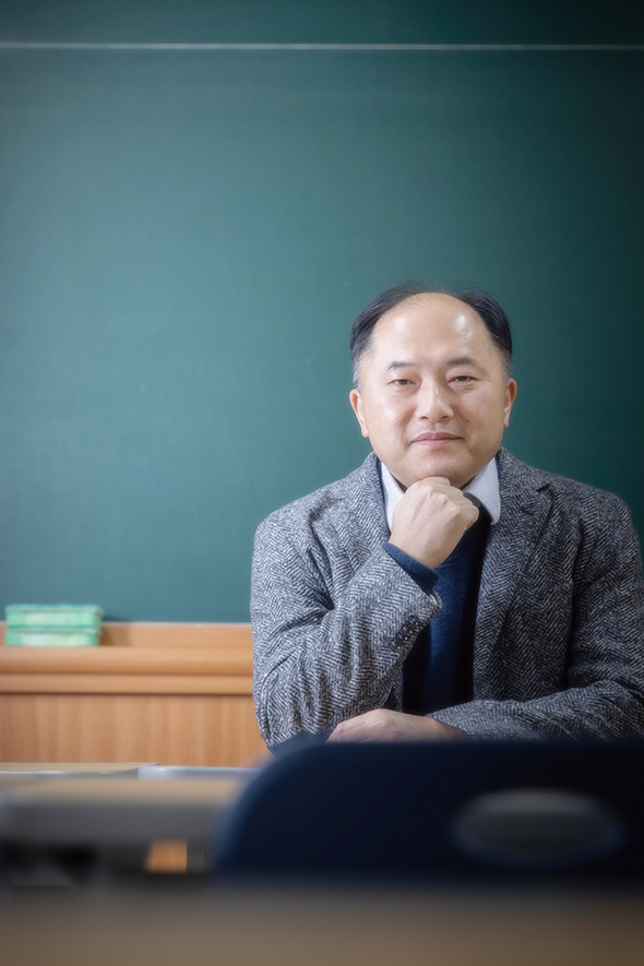
한양인터칼리지 ‘미래반도체공학전공’ 정문석 교수(물리학과)
Professor Jeong Mun Seok,
“Major in Semiconductor Engineering Future” at Hanyang Intercollege
(Department of Physics)
- 글 박영임
- 사진 손초원
- Writing Park Young-im
- Photograph Son Cho-won
Scroll Down
4차 산업혁명 시대의 핵심 동력인 반도체 산업은 이제 국가 경쟁력 강화를 위해서도 필수적인 산업이 됐다. 하지만 기존의 교육 시스템은 산업 수요를 빠르게 반영하지 못하고 있다. 전자공학, 신소재공학, 기계공학, 물리학 등 학문 간 경계를 허문 한양인터칼리지 미래반도체공학전공은 융합형 반도체 인재 육성을 목표로 한다.
The semiconductor industry, a core driving force of the Fourth Industrial Revolution era, has now become an essential industry for strengthening national competitiveness. However, existing education systems have failed to quickly reflect industry demands. The Major in Semiconductor Engineering Future at Hanyang Intercollege, which has broken down boundaries between disciplines such as electronic engineering, materials science and engineering, mechanical engineering, and physics, aims to cultivate convergence-oriented semiconductor talents.
반도체 산업의 다음 스텝을 고민하다
“AI 기술의 촉발로 다양한 분야에서 반도체 수요가 폭발적으로 증가하고 있습니다. 예를 들어 완전한 자율주행차를 위해서는 초고성능 슈퍼컴퓨터 반도체 성능이 요구되는데, 그러려면 반도체 성능이 지금보다 천 배 정도는 증가해야 합니다. 정점에 이른 현 반도체 기술의 한계를 넘어서려면 패러다임의 전환이 시급합니다.”
미래반도체공학전공 주임교수인 정문석 교수는 미래의 반도체 기술은 현재의 수준을 뛰어넘는 ‘비욘드 커런트 테크놀로지(Beyond Current Technology)’를 의미한다고 강조했다. 한양대학교 반도체 산학협력체인 한양스마트반도체연구원(HY-ISS) 산하 차세대반도체물성및소자연구센터(CSPD)의 센터장이자 첨단반도체부트캠프의 부단장으로서 반도체 산업을 면밀히 파악해 온 이의 말이라 더 깊게 와닿는다.
“과학 저널리스트인 매트 리들리(Matt Ridley)는 그의 저서에서 혁신은 다양한 아이디어가 융합할 때 나온다고 했습니다. 다학제적 교육, 특히 기초과학과 공학의 용광로 같은 융합만이 새로운 반도체 패러다임을 제시할 수 있다고 생각합니다.”
단순한 기술 개발을 넘어 창의적인 문제 해결법을 제시하려면 본질을 파헤쳐 혁신의 단초를 찾아야 한다. 그렇기에 미래반도체공학전공은 기초학문 교육에도 힘을 쏟는다. ‘기초 반도체 물리(2학년)’나 ‘반도체 고체 물리학 개론(3학년)’ 등 물리학 기반의 과목들을 포함하여 교육과정을 구성했다. 이러한 교육과정을 통해 새로운 개념의 반도체 소재 및 소자 구조에 대한 가능성을 탐구하고, 나아가 실제 활용 가능성을 제시하는 것이 미래반도체공학전공이 추구하는 교육 방향이다.
Contemplating the Next Step for the Semiconductor Industry
“The advent of AI technology has triggered an explosive increase in semiconductor demand across various fields. For example, fully autonomous vehicles require ultra-high-performance supercomputer-level semiconductor performance, which means semiconductor performance needs to increase about a thousand times compared to current levels. To surpass the limits of current semiconductor technology that has reached its peak, a paradigm shift is urgently needed.”
Professor Jeong Mun Seok, program director of the Major in Semiconductor Engineering Future, emphasized that future semiconductor technology means “Beyond Current Technology”—surpassing present levels. His words resonate deeply as a researcher who has closely examined the semiconductor industry in his roles as Director of the Center for Semiconductor Physics and Devices (CSPD) under Hanyang University's semiconductor industry-academia cooperation body, the Hanyang Institute of Smart Semiconductor (HY-ISS), and as Deputy Director of the Advanced Semiconductor Bootcamp.
“Science journalist Matt Ridley stated in his book that innovation emerges when diverse ideas converge. I believe that only multidisciplinary education—particularly a melting pot-like convergence of basic science and engineering—can present a new semiconductor paradigm.”
To present creative problem-solving methods beyond simple technology development, one must delve into the essence to find the seeds of innovation. That is why the Major in Semiconductor Engineering Future also focuses on fundamental academic education. The curriculum includes physics-based courses such as “Basic Semiconductor Physics” (sophomore year) and “Introduction to Semiconductor Solid-State Physics” (junior year). Through this curriculum, the educational direction pursued by the Major in Semiconductor Engineering Future is to explore the possibilities of new-concept semiconductor materials and device structures, and furthermore, to present their practical application potential.
정문석 교수는 기초과학과 공학의 용광로 같은 융합만이 새로운 반도체 패러다임을 제시할 수 있다며, 학생들의 기초학문 교육에 힘쓰는 이유를 설명했다.
Professor Jeong Mun Seok explained that only a melting pot-like convergence of basic science and engineering can present a new semiconductor paradigm, which is why he is committed to educating students in fundamental disciplines.
반도체 전 영역에 대한 융합 교육 및 실습 시행
이와 더불어 반도체 공정, 역학, 회로, 패키징, 설계 등 학문 간 장벽을 허물어 반도체 전 영역에 대한 융합 교육을 실시한다. 여기에 인공지능 및 머신러닝 활용에 이르기까지, 최신 기술 교육과정도 발 빠르게 반영했다. 그러나 미래반도체공학전공은 단순히 융합형 인재 양성에 만족하지 않는다. 졸업 후 현장에 바로 투입될 수 있는 실무형 인재를 목표로 한다. 그래서 반도체 8대 공정에 대한 실험·실습, 반도체 소자 및 패키징을 직접 설계하고 테스트할 수 있는 실험·실습 수업이 중심이 된다.
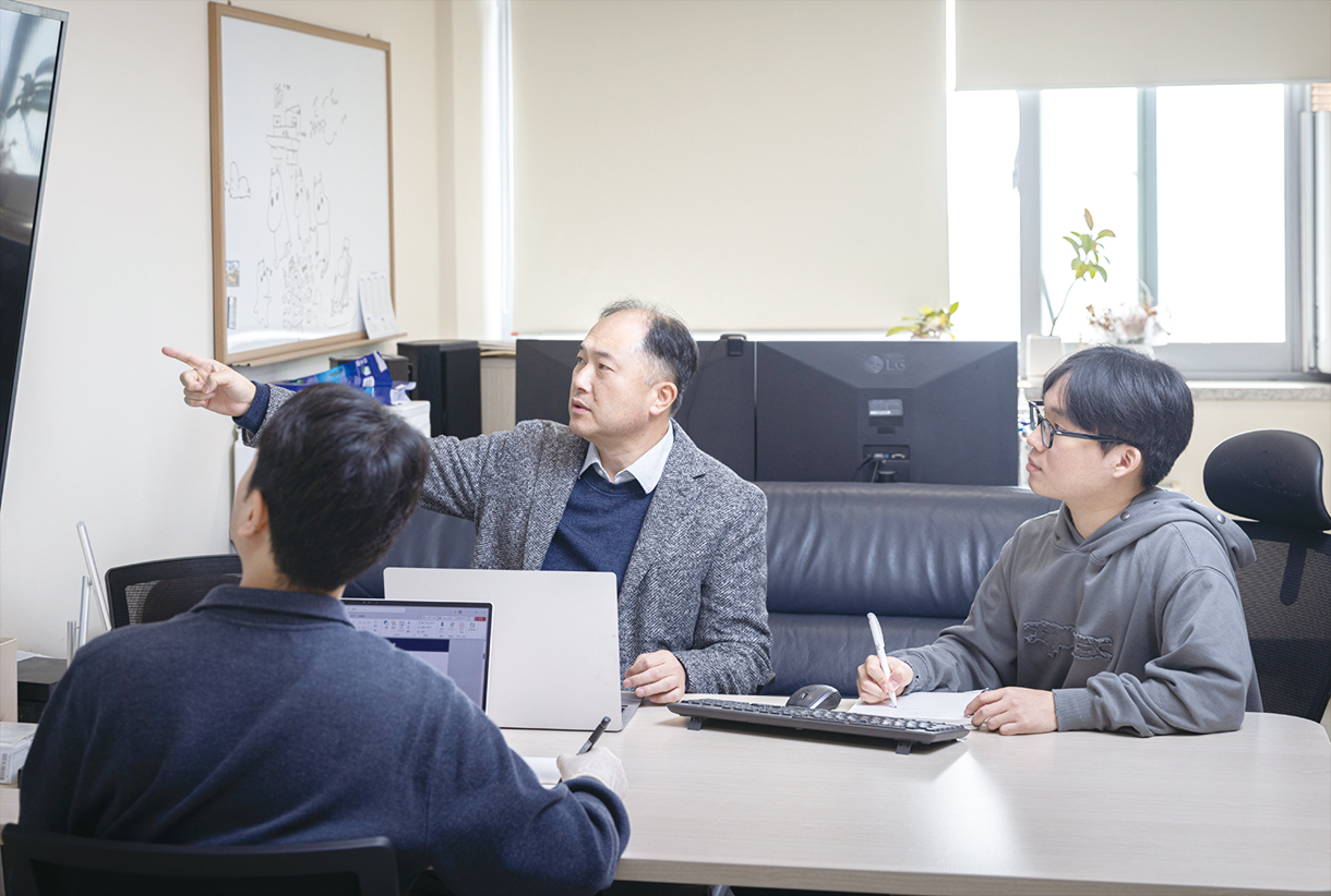
이러한 반도체 실험·실습 교육을 진행하기에 한양대는 최적의 인프라를 갖추고 있다. 국내 최고 수준의 반도체 팹(Fab)과 패키징 팹 시설을 구축하고 있기 때문이다. 이에 추가적으로 반도체 물성 분석 및 소자 제작 실습에 특화된 실습실도 준비 중이다. 실습실에는 학부 과정의 실습 교육은 물론, 대학원 과정의 연구까지 가능한 고성능 실습장비들을 구축할 예정이다. 실력을 갖춘 학생들은 실습실을 기반으로 3학년 때부터 학부연구생으로 교수들의 연구 프로젝트에 참여해 대학원 수준의 실습 경험을 쌓고, 4학년 때는 학회에서 논문 발표도 하게 된다.
“학부생을 연구에 참여시키는 것은 조기에 전문 인재를 육성하기 위해서입니다. 학·석 연계 과정이나 석·박사 통합 과정 등을 활용해 산업 현장에서 필요로 하는 반도체 전문 연구원을 빠르게 배출하려 합니다.”
Implementing Convergence Education and Practical Training Across All Semiconductor Fields
In addition, convergence education across all semiconductor fields is conducted by breaking down interdisciplinary barriers in semiconductor processing, mechanics, circuits, packaging, and design. The latest technology curricula, including artificial intelligence and machine learning applications, have also been quickly incorporated. However, the Major in Semiconductor Engineering Future is not satisfied with simply cultivating convergence talents. It aims to cultivate practice-oriented talents who can work in the field right after graduation. Therefore, laboratory and practicum courses centered on experiments and hands-on training in the eight major semiconductor processes, as well as direct design and testing of semiconductor devices and packaging, form the core of the program.
Hanyang University possesses optimal infrastructure for conducting such semiconductor laboratory and practical training education. This is because it has established semiconductor fab and packaging fab facilities at the highest level in Korea. Additionally, a laboratory specialized in semiconductor property analysis and device fabrication training is being prepared. The laboratory will be equipped with high-performance training equipment capable of supporting not only undergraduate practicum education but also graduate-level research. Qualified students, based on this laboratory, will participate as undergraduate researchers in professors' research projects starting from their junior year to gain graduate-level hands-on experience, and present papers at academic conferences in their senior year.
“The reason for involving undergraduate students in research is to cultivate specialized talents at an early stage. We aim to quickly cultivate semiconductor specialist researchers demanded in the industrial field by utilizing combined bachelor's-master's programs or integrated master's-doctoral programs.”
한양인터칼리지 미래반도체공학전공은 다학제적 교육과 실무 중심의 연구 역량 육성 과정으로 짜여 있다
The Major in Semiconductor Engineering Future at Hanyang Intercollege is structured as a multidisciplinary education and practice-centered research capability development program.
융합의 힘으로 새 시대 열 주역 되길
더불어 3학년 과정부터 ‘반도체 고체 물리학 개론’을 제외한 전 과목을 IC-PBL 수업으로 진행한다. 즉, 반도체 기업들과 협력해 실제 산업체가 당면한 과제에 대한 솔루션을 직접 제시하는 팀 프로젝트나 세미나로 현장 전문가들과 호흡할 기회를 확대할 계획이다.
이렇게 미래반도체공학전공은 다학제적 교육과 실무 중심의 연구 역량 육성 과정으로 짜여 있다. 반도체 산업이 요구하는, 반도체 전 분야에 대한 통합적 이해와 문제해결 능력을 갖춘 인재를 양성하기 위해서다. 정문석 교수는 미래반도체공학전공이 글로벌 반도체 산업을 이끌 창의적인 융합형 인재 배출에 이바지할 것이리라 자신했다. 그리고 한양인에게 다음과 같이 당부했다.
“문제를 스스로 정의하고 해결할 수 있는 융합형 인재가 그 어느 때보다 절실합니다. 그를 위해서는 기초학문부터 응용기술에 이르는 지식의 폭과 깊이를 갖추고, 새로운 것을 두려워하지 않는 도전정신이 필요해요. 우리가 배운 물리학 이론이 내일의 반도체 기술이 되고, 오늘의 실습에서 얻은 작은 통찰이 미래 산업의 문을 여는 열쇠가 될 수 있어요. 변화의 중심에 서고 싶은 한양인이라면 스스로에게 묻고, 스스로 답을 찾는 사람으로 성장하길 바랍니다. 끊임없이 배우고 연결하며 융합의 힘으로 새로운 시대를 열어갈 주역이 되길 기대하겠습니다.”
Becoming the Leaders Who Will Open a New Era Through the Power of Convergence
Furthermore, starting from the junior year, all courses except “Introduction to Semiconductor Solid-State Physics” will be conducted as IC-PBL (Industry-Coupled Problem-Based Learning) classes. In other words, the plan is to expand opportunities to collaborate with field experts through team projects and seminars that directly propose solutions to challenges faced by actual industries in cooperation with semiconductor companies.
In this way, the Major in Semiconductor Engineering Future is structured as a multidisciplinary education and practice-centered research capability development program. This is to cultivate talents equipped with comprehensive understanding across all semiconductor fields and problem-solving abilities that the semiconductor industry demands. Professor Jeong Mun Seok expressed confidence that the Major in Semiconductor Engineering Future at Hanyang Intercollege will contribute to producing creative convergence talents who will lead the global semiconductor industry. He also offered the following message to Hanyang people.
“Convergence talents who can define and solve problems on their own are more urgently needed than ever. To achieve this, one must profoundly and widely explore knowledge ranging from fundamental academics to applied technologies and have a challenging spirit that is not afraid of new things. The physics theories we learn can become tomorrow's semiconductor technology, and the small insights gained from today's practicum can become the key to opening the doors of future industries. If you are a Hanyang person who wants to stand at the center of change, I hope you will grow into someone who asks questions and finds answers on your own. I look forward to you becoming leaders who will open a new era through the power of convergence by continuously learning and connecting.”
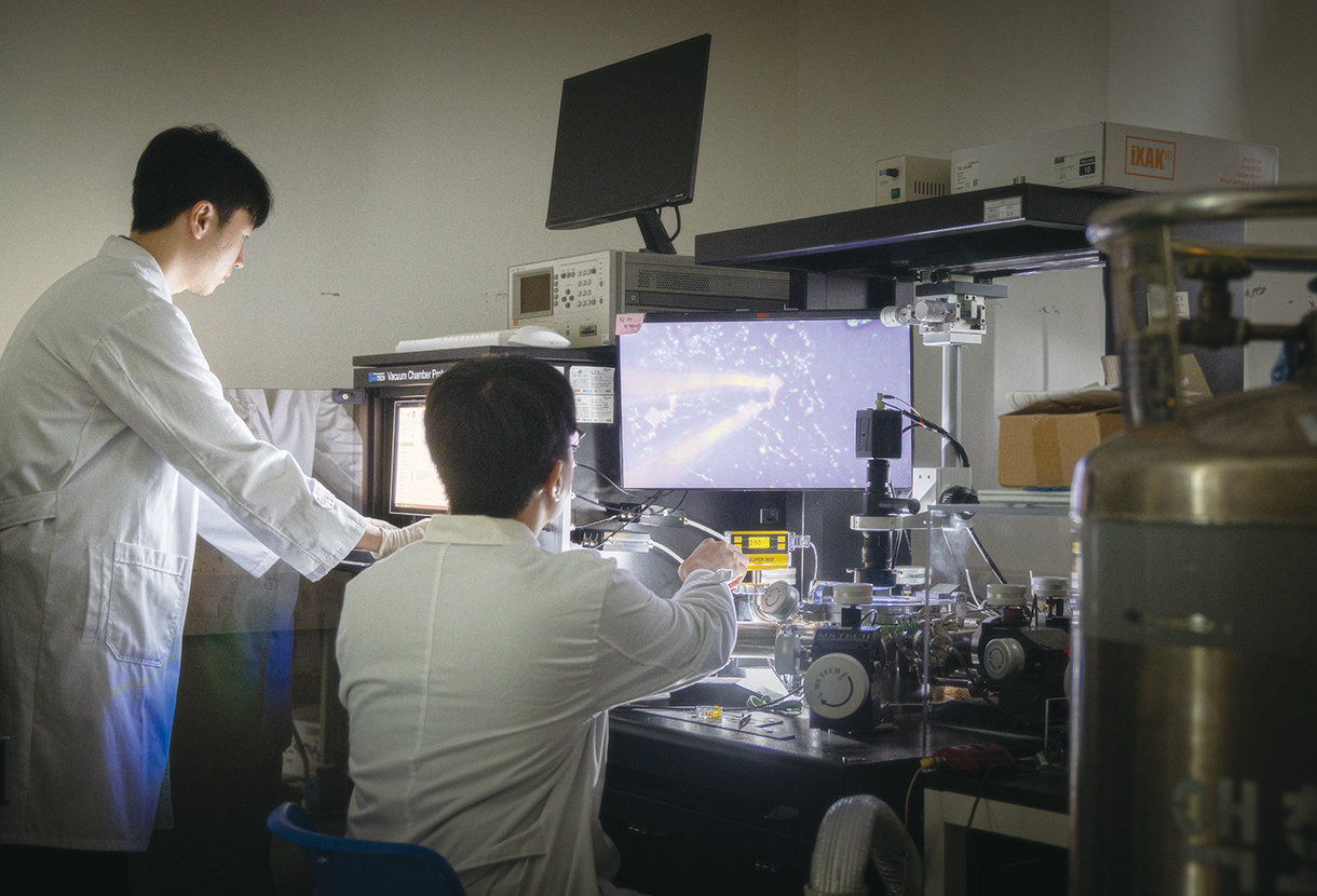
미래반도체공학전공은 융합 역량을 갖추고, 졸업 후 현장에 바로 투입될 수 있는 실무형 인재를 양성하고자 한다. 사진은 반도체 공정에 대한 실험·실습 모습.
The Major in Semiconductor Engineering Future aims to cultivate practice-oriented convergence talents who can work in the field right after graduation. The photo shows students conducting experiments and hands-on training in semiconductor processing.